
February 24th 15:30-17:30 @ IVA Konferenscenter:
The seminar’s keynote lecture will be delivered by Professor Tsunenobu Kimoto, Kyoto University; Unlocking Power Efficiency: The Rise and Impacts of SiC Semiconductor Technology.
Details & Registration: https://www.iva.se/en/what-iva-does/events/top-scientist-lecture-on-semiconductors/
The seminar is also broadcasted OnLine. Participation: Online: Free. On Location: Free
Recent disruptions in global supply chains and rapid technological progress have underscored the strategic importance of strong research capabilities, industrial scale-up and international collaboration. Japan has emerged as a leading actor in advanced semiconductor technologies and is making major investments to strengthen competitiveness across research, manufacturing and innovation ecosystems.
Against this backdrop, this seminar brings together leading researchers and industry experts from Japan and Sweden to discuss advances in next-generation semiconductor technologies, industrial development, and the role of international collaboration in driving innovation, resilience, and long-term technological leadership.
The Top Scientist Lecture seminar is a recurring collaboration between JSPS – Japan Society for the Promotion of Science, the Japanese Embassy, SJF (Sweden Japan Foundation) and IVA. With support from SSF – The Swedish Foundation for Strategic Research.
About Prof Kimoto:
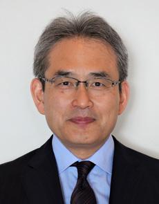
Professor Tsunenobu Kimoto is a Japanese electrical engineer and a professor at the Graduate School of Engineering, Kyoto University, where he leads the Semiconductor Science and Engineering (Kimoto) Laboratory.
His research focuses on wide-bandgap semiconductor materials, especially silicon carbide (SiC), including crystal growth, characterization, and the development of high‑performance SiC power devices and interfaces such as SiC MOS structures. He played a central role in establishing fundamental technologies for SiC power semiconductors—such as high‑quality epitaxial growth, defect reduction, ion implantation, and precise characterization of key material parameters—which have been widely adopted for high‑efficiency power electronics in applications like railways and electric vehicles.